- 您现在的位置:买卖IC网 > Sheet目录3826 > PIC18F4455-I/ML (Microchip Technology)IC PIC MCU FLASH 12KX16 44QFN
PIC18F2455/2550/4455/4550
DS39632E-page 168
2009 Microchip Technology Inc.
There are 6 signals from the module to communicate
with and control an external transceiver:
VM: Input from the single-ended D- line
VP: Input from the single-ended D+ line
RCV: Input from the differential receiver
VMO: Output to the differential line driver
VPO: Output to the differential line driver
UOE: Output enable
The VPO and VMO signals are outputs from the SIE to
the external transceiver. The RCV signal is the output
from the external transceiver to the SIE; it represents
the differential signals from the serial bus translated
into a single pulse train. The VM and VP signals are
used to report conditions on the serial bus to the SIE
that can’t be captured with the RCV signal. The
combinations of states of these signals and their
interpretation are listed in Table 17-1 and Table 17-2.
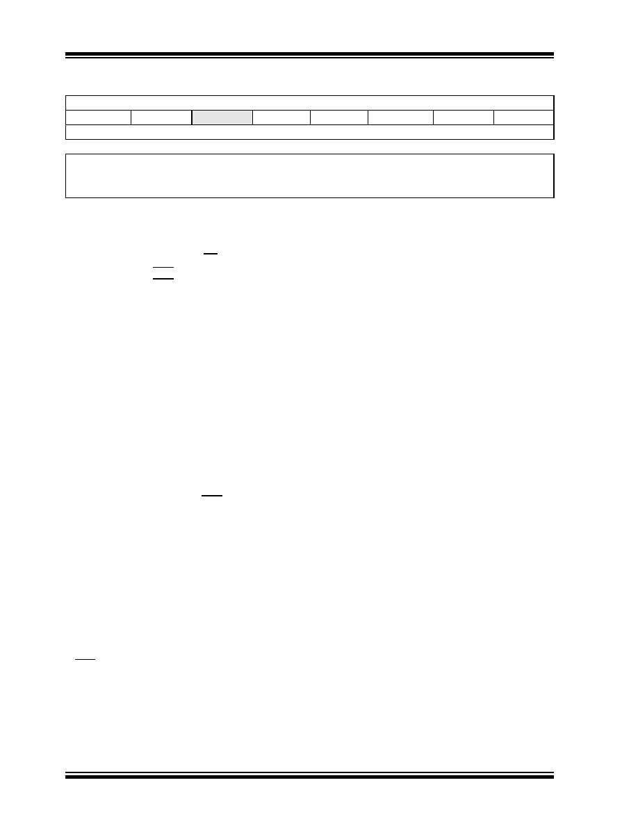
REGISTER 17-2:
UCFG: USB CONFIGURATION REGISTER
R/W-0
U-0
R/W-0
UTEYE
UOEMON(1)
—
UPUEN(2,3)
UTRDIS(2)
FSEN(2)
PPB1
PPB0
bit 7
bit 0
Legend:
R = Readable bit
W = Writable bit
U = Unimplemented bit, read as ‘0’
-n = Value at POR
‘1’ = Bit is set
‘0’ = Bit is cleared
x = Bit is unknown
bit 7
UTEYE: USB Eye Pattern Test Enable bit
1 = Eye pattern test enabled
0 = Eye pattern test disabled
bit 6
UOEMON: USB OE Monitor Enable bit(1)
1 =UOE signal active; it indicates intervals during which the D+/D- lines are driving
0 =UOE signal inactive
bit 5
Unimplemented: Read as ‘0’
bit 4
UPUEN: USB On-Chip Pull-up Enable bit(2,3)
1 = On-chip pull-up enabled (pull-up on D+ with FSEN = 1 or D- with FSEN = 0)
0 = On-chip pull-up disabled
bit 3
UTRDIS: On-Chip Transceiver Disable bit(2)
1 = On-chip transceiver disabled; digital transceiver interface enabled
0 = On-chip transceiver active
bit 2
FSEN: Full-Speed Enable bit(2)
1 = Full-speed device: controls transceiver edge rates; requires input clock at 48 MHz
0 = Low-speed device: controls transceiver edge rates; requires input clock at 6 MHz
bit 1-0
PPB1:PPB0: Ping-Pong Buffers Configuration bits
11 = Even/Odd ping-pong buffers enabled for Endpoints 1 to 15
10 = Even/Odd ping-pong buffers enabled for all endpoints
01 = Even/Odd ping-pong buffer enabled for OUT Endpoint 0
00 = Even/Odd ping-pong buffers disabled
Note 1:
If UTRDIS is set, the UOE signal will be active independent of the UOEMON bit setting.
2:
The UPUEN, UTRDIS and FSEN bits should never be changed while the USB module is enabled. These
values must be preconfigured prior to enabling the module.
3:
This bit is only valid when the on-chip transceiver is active (UTRDIS = 0); otherwise, it is ignored.
发布紧急采购,3分钟左右您将得到回复。
相关PDF资料
PIC24FJ64GB108-I/PT
IC PIC MCU FLASH 80TQFP
DSPIC33FJ64MC506A-I/PT
IC DSPIC MCU/DSP 64K 64-TQFP
PIC16F877A-I/P
IC MCU FLASH 8KX14 EE 40DIP
MP2-HS240-51
CONN SHROUD 2-FB 240POS 5ROW
DSPIC33FJ64MC506-I/PT
IC DSPIC MCU/DSP 64K 64TQFP
DSPIC33FJ128MC802-I/SO
IC DSPIC MCU/DSP 128K 28SOIC
PIC18LF4331-I/P
IC PIC MCU FLASH 4KX16 40DIP
DSPIC33FJ128GP306-I/PT
IC DSPIC MCU/DSP 128K 64TQFP
相关代理商/技术参数
PIC18F4455-I/P
功能描述:8位微控制器 -MCU 24kBF 2048RM FSUSB2 RoHS:否 制造商:Silicon Labs 核心:8051 处理器系列:C8051F39x 数据总线宽度:8 bit 最大时钟频率:50 MHz 程序存储器大小:16 KB 数据 RAM 大小:1 KB 片上 ADC:Yes 工作电源电压:1.8 V to 3.6 V 工作温度范围:- 40 C to + 105 C 封装 / 箱体:QFN-20 安装风格:SMD/SMT
PIC18F4455-I/PT
功能描述:8位微控制器 -MCU 24kBF 2048RM FSUSB2 RoHS:否 制造商:Silicon Labs 核心:8051 处理器系列:C8051F39x 数据总线宽度:8 bit 最大时钟频率:50 MHz 程序存储器大小:16 KB 数据 RAM 大小:1 KB 片上 ADC:Yes 工作电源电压:1.8 V to 3.6 V 工作温度范围:- 40 C to + 105 C 封装 / 箱体:QFN-20 安装风格:SMD/SMT
PIC18F4455T-I/ML
功能描述:8位微控制器 -MCU 24kBF 2048RM FSUSB2 RoHS:否 制造商:Silicon Labs 核心:8051 处理器系列:C8051F39x 数据总线宽度:8 bit 最大时钟频率:50 MHz 程序存储器大小:16 KB 数据 RAM 大小:1 KB 片上 ADC:Yes 工作电源电压:1.8 V to 3.6 V 工作温度范围:- 40 C to + 105 C 封装 / 箱体:QFN-20 安装风格:SMD/SMT
PIC18F4455T-I/PT
功能描述:8位微控制器 -MCU 24kBF 2048RM FSUSB2 RoHS:否 制造商:Silicon Labs 核心:8051 处理器系列:C8051F39x 数据总线宽度:8 bit 最大时钟频率:50 MHz 程序存储器大小:16 KB 数据 RAM 大小:1 KB 片上 ADC:Yes 工作电源电压:1.8 V to 3.6 V 工作温度范围:- 40 C to + 105 C 封装 / 箱体:QFN-20 安装风格:SMD/SMT
PIC18F4458-I/ML
功能描述:8位微控制器 -MCU 24KB Flash 2KB RAM RoHS:否 制造商:Silicon Labs 核心:8051 处理器系列:C8051F39x 数据总线宽度:8 bit 最大时钟频率:50 MHz 程序存储器大小:16 KB 数据 RAM 大小:1 KB 片上 ADC:Yes 工作电源电压:1.8 V to 3.6 V 工作温度范围:- 40 C to + 105 C 封装 / 箱体:QFN-20 安装风格:SMD/SMT
PIC18F4458-I/P
功能描述:8位微控制器 -MCU 24KB Flash 2KB RAM RoHS:否 制造商:Silicon Labs 核心:8051 处理器系列:C8051F39x 数据总线宽度:8 bit 最大时钟频率:50 MHz 程序存储器大小:16 KB 数据 RAM 大小:1 KB 片上 ADC:Yes 工作电源电压:1.8 V to 3.6 V 工作温度范围:- 40 C to + 105 C 封装 / 箱体:QFN-20 安装风格:SMD/SMT
PIC18F4458-I/PT
功能描述:8位微控制器 -MCU 24KB Flash 2KB RAM RoHS:否 制造商:Silicon Labs 核心:8051 处理器系列:C8051F39x 数据总线宽度:8 bit 最大时钟频率:50 MHz 程序存储器大小:16 KB 数据 RAM 大小:1 KB 片上 ADC:Yes 工作电源电压:1.8 V to 3.6 V 工作温度范围:- 40 C to + 105 C 封装 / 箱体:QFN-20 安装风格:SMD/SMT
PIC18F4458T-I/ML
功能描述:8位微控制器 -MCU 24KB Flash 2KB RAM RoHS:否 制造商:Silicon Labs 核心:8051 处理器系列:C8051F39x 数据总线宽度:8 bit 最大时钟频率:50 MHz 程序存储器大小:16 KB 数据 RAM 大小:1 KB 片上 ADC:Yes 工作电源电压:1.8 V to 3.6 V 工作温度范围:- 40 C to + 105 C 封装 / 箱体:QFN-20 安装风格:SMD/SMT